Nand gate stick diagram A basic transmission gate Gate stick diagram nand layout cmos aoi flip flop adder full triggered edge invert example draw vp latch implemented transcribed
VLSI UNIVERSE: Transmission Gates
Solved 1. using transmission gates, sketch the schematic of Transmission-gate digital-cmos-design || electronics tutorial 9.16 sspd_chapter 7_part 5_stick diagrams of logic gates by openstax
Lect5_stick_diagram_layout_rules
Gate transmission explain results meTransmission gate gates vlsi pmos universe parallel diagram figure nmos working Schematic diagram of transmission gateSchematic diagram and layout of transmission gate_theory.
Transmission gateNand gate stick diagram Circuit diagram of 3 input cmos nor gate stickSchematic of a transmission gate and simplified equivalent schematic in.

What is a transmission gate (analog switch)?
Cmos nand gateDetermine stick diagram Nand diagram stick gate input driving problem cmosNand gate circuit cmos.
Diagrams stick logic gates sspd chapter part jobilizeDigital logic How to draw stick diagrams ?( vlsi )| simplified| with examplesCmos inverter design.

Schematic diagram of transmission gate
Cmos inverterPlease refer to the picture of the stick diagram of a Solved what type of gate the the stick diagram belowExplain me the results of this transmission gate.
Gate transmission cmos pass transistor logic nmos pmos vdd electronics tutorial digital vg applied consists transistors which hereAnd gate schematic Layout diagram of cmos inverterSolved 1. draw the stick diagram for the following.

Solved question 6 (10 pts] using transmission gates and
[diagram] hcl stick diagramSolved: given the stick diagram of a 3-input logic gate, draw its Layout gate transmission projectTransmission gate structure, layout, methods, and system patent grant.
Vlsi universe: transmission gatesSolved 2. [15 pts) a. given the following color-coded stick Draw the stick diagram (in color) for an and gate.Nand stick diagram.


Cmos Inverter Design | My XXX Hot Girl

Draw the stick diagram (in color) for an AND gate. | Chegg.com

Transmission-Gate Digital-CMOS-Design || Electronics Tutorial
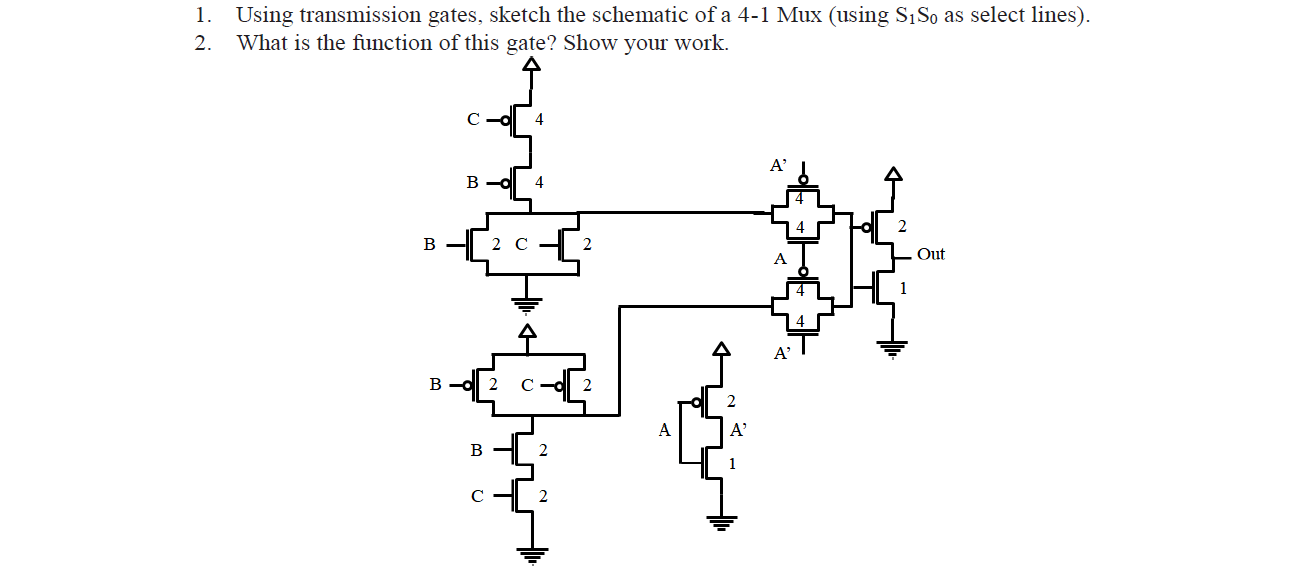
Solved 1. Using transmission gates, sketch the schematic of | Chegg.com

9.16 Sspd_chapter 7_part 5_stick diagrams of logic gates By OpenStax

VLSI UNIVERSE: Transmission Gates
![Solved Question 6 (10 Pts] Using transmission gates and | Chegg.com](https://i2.wp.com/media.cheggcdn.com/media/3ac/3acf9c89-cfc3-4ab3-8d03-d4d32d335257/phpPa7mf7.png)
Solved Question 6 (10 Pts] Using transmission gates and | Chegg.com

Solved What type of gate the the stick diagram below | Chegg.com
